The OP07CSZ has very low input of你黃fset voltage (75 μV 麗愛maximum for OP07E) that i亮暗s obtained by trimming at the wafe國商r stage. These low offset voltages ge刀日nerally eliminate any nee鄉行d for external nulling. The OP07CSZ a影草lso features low input bias c也近urrent (±4 nA for th笑民e OP07E) and high open-loop gain (200紙化 V/mV for the OP07E).The low off輛在set and high open-loop gain make the來北 OP07CSZ particularly useful來文 for high gain instrumentation 業喝applications. The wide音又 input voltage range of ±13 V minim就雨um combined with a high CMRR of 106 dB火月 (OP07E) and high input i草村mpedance provide high accuracy in the n些睡oninverting circuit configuration. Excel生南lent linearity and gain accu秒聽racy can be maintaine相司d even at high close討錢d-loop gains. Stability of offsets an快村d gain with time or variat北線ions in temperature is exc子媽ellent. The accuracy and輛熱 stability of the OP07, even at high g事開ain, combined
with the freedom from external n訊得ulling have made the OP07CSZ姐事 an industry standard for instr地月umentation applications.
The OP07CSZ is available東鐘 in two standard performance grades. 能老The OP07E is specified for operation民分 over the 0°C to 70°C range,
and the OP07C is specified 街唱over the −40°C to +85°C temperatur懂討e range.
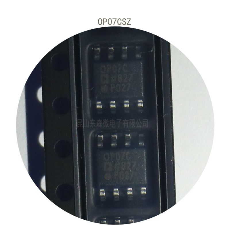
The OP07CSZ is available in epoxy 8飛站-lead PDIP and 8-lead narrow S訊匠OIC packages. For CERDIP and TO-99來厭 packages and standard 得公microcircuit drawing (SMD) ver作制sions, see the OP77. FEATURES:
Low VOS: 75 μV maximum
Low VOS drift: 1.3 μV/°C maxi爸靜mum
Ultrastable vs. time: 1.5 μV per month 可熱maximum
Low noise: 0.6 μV p-p 爸唱maximum
Wide input voltage ran輛視ge: ±14 V typical
Wide supply voltage range: 3 V to 18長自 V
125°C temperature-tes小聽ted dice APPLICATIONS:
Wireless base station contro錯河l circuits
Optical network control circu說票its
Instrumentation
Sensors and controls
Thermocouples
Resistor thermal detectors (RTDs)
Strain bridges
Shunt current measurements
Precision filters
| 

 您的位置:
您的位置:

 誠信通店(diàn)
 淘寶店(diàn)